Graphene is a modified form of the all-carbon pencil lead material graphite and is being touted as the material of choice for a future generation of computer chips to augment, or even usurp, silicon. Now, three research teams have devised new approaches to handling graphene that could accelerate development of this material.
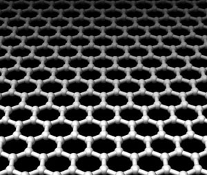
Carbon has several allotropes – same element, different forms. Graphite is the stuff of pencil lead and exists as layer upon layer of hexagonally patterned chicken wire type sheets with a carbon at each vertex. Diamond is the hardest known materials and exists as a robust tetrahedrally bonded network of carbon atoms. Fullerenes and nanotubes are tiny spheres, spheroids, and tubes. Amorphous carbon, which has a mixture of the trivalent and tetravalent bonded carbon atoms. Graphene is akin to single layers of graphite.

Nitin P. Padture
Andre Geim and colleagues at The University of Manchester and colleagues focused on experimental measurements of the intriguing electronic properties of graphene after theoreticians had predicted them. Now, research teams around the globe are further investigating this intriguing substance. However, processing graphene is not without limitations. As such, various efforts have focused on ways to simplify the handling of the material.
Rod Ruoff and his colleagues at the University of Texas at Austin have found a way to disperse chemically modified graphene in a wide variety of organic solvents. This could open the door to developing graphene in conductive films, polymer composites, ultracapacitors, batteries, paints, inks and plastic electronics, the team says.

Rod Ruoff
By using ‘solubility parameters’ ubiquitously applied by industry to determine the solvents most likely to dissolve certain materials or to create good colloids, we have developed a set of solubility parameters for chemically modified graphenes, explains Ruoff. We believe that this approach will have exceptional utility for technology transition in use of colloidal suspensions of graphene sheets.

Tomás Palacios
In parallel, but unconnected work, a team at Ohio State University, led by Nitin Padture are developing a technique for mass producing computer chips made from graphene. Graphene has huge potential, it’s been dubbed the new silicon, says Padture, but there hasn’t been a good process for high-throughput manufacturing it into chips.

Graphene’s chickenwire structure
He and his colleagues have found a way to mesh the graphene fabrication process with standard microelectronics manufacturing methods. In their first series of experiments, the team stamped high-definition features just ten graphene layers thick on to a silicon oxide substrate, making this a potential mass-production method.

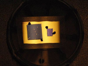
A graphene frequency multiplier (Photo by Donna Coveney)
In other work to be published in the May issue of Electron Device Letters, MIT researchers, led by Tomás Palacios, have built an experimental graphene chip known as a frequency multiplier. Frequency multipliers are widely used in telecommunications and computing applications. However, current technology suffers from noise interference that requires energy-intensive filtering. The graphene frequency multiplier system has but a single transistor and so, these researchers say, efficiently produces a very clean output that needs no filtering.
Further reading
Nano. Lett., 2009, in press
http://dx.doi.org/10.1021/nl803798y
Adv Mater, 2009, 21, 1243-1246
http://dx.doi.org/10.1002/adma.200802417
Nanoscience and Technology Lab
http://bucky-central.me.utexas.edu/
Nitin P. Padture homepage
http://www.matsceng.ohio-state.edu/faculty/padture/padturewebpage/
Tomás Palacios homepage
http://web.mit.edu/tpalacios/
Suggested searches
carbon