Anyone who enjoys a delicious bowl of mixed grain Cheerios in the morning, rather than being force-fed lumpy porridge, will know all about the Cheerios Effect. This phenomenon is usually manifest at a particular point during breakfast when just a few torus-shaped Cheerios are left floating on the milk. Minor agitation of this mixed-phase, composite system will cause individual Cheerios to bump into each other and to form aggregate complexes.
This amazing scientific phenomenon is due to the surface tension of the milk, which is essentially an emulsion of fats and proteins in water. The effect was only recently reported in the scientific literature and ranks alongside, other surface tension phenomena including the ability of water to migrate from one end to the other of a thin tube, capillary action, the ability of some aquatic insects, such as pond skaters, to walk on the surface of water, and the recent discovery of liquid marbles, which can be formed by powder coating solvent droplets.

Dr Steven E J Bell
Now, Steven Bell of Queen’s University Belfast has combined his team’s expertise in superhydrophobic materials, discussed previously in Spotlight, to enable a rather novel demonstration of the Cheerios Effect on a much smaller scale with potential technological applications.
The researchers coated microscopic particles of copper metal with their superhydrophobic material. When you pour these particles on to water they float because of their powerful water repellency, or hydrophobicity, despite the density of the copper. However, they gradually assemble into really strong sheets because of the ‘Cheerios Effect’, which is really powerful in this case, explains Bell. The high density of the particles bend the meniscus, the surface of the water, significantly.

A sugar cube coated with the particles can be held under water without dissolving (Image courtesy of Iain Larmour)
Bell and his colleagues have uploaded two videos to YouTube showing the microscopic Cheerios Effect in action. One video shows the spontaneous coalescence of the particles, the other demonstrates just how strong it is with a view of the flat end of a pencil being pushed through a layer of particles and into the water. One can see that no water is absorbed on to the surface of the pencil, which is not the case when a pencil is dipped into water without the superhydrophobic layer. Other phenomena include the protection of a sugar cube from dissolving in water and the supporting of other objects on the surface of water.

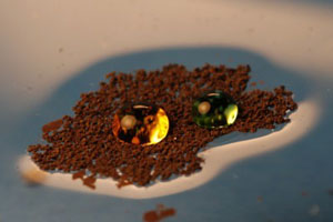
Two coloured water drops sitting on an assembled superhydrophobic sheet, gaps between the particles are obvious but the water does not fall through (Image courtesy of Iain Larmour)
The most striking property of the sheets is the extent to which they can support objects, Bell says, sheets composed of either small (less than 75 micrometres) or large (less than 400 micrometres) particles can support the weight of water droplets indefinitely and even irregular, relatively large fragments of cement.

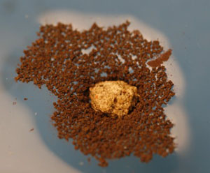
A cement fragment supported by the larger superhydrophobic copper particles (Image courtesy of Iain Larmour)
Bell adds that, The superhydrophobic copper particle sheets support objects because they satisfy two linked criteria: First, the particles in the sheet have sufficient buoyancy to support the external load. Secondly, under loading conditions the sheets do not tear or develop holes which are large enough for the supported object to contact the water beneath. Preventing this contact is important, because as soon as it occurs the supported objects fall through the sheet.
The particles may one day have technological applications, but at the moment, Bell and colleagues are optimizing the shape of the particles to make stronger sheets. They are also using their materials as a macroscale model of the microscopic phenomenon of emulsification, in which tiny, colloidal particles suspended in a liquid form a stable mixture that never settles, as occurs in milk.
Working with Iain Larmour and Graham Saunders, Bell has now published details of the work in the chemistry journal Angewandte Chemie with the title: Self Assembled on Water by the Cheerios Effect. I always wanted to get the name of a breakfast cereal into the title of a serious research paper, Bell told Spotlight.
Further reading
Angew Chem Int Edn, 2008, 47, 5043-5045
http://dx.doi.org/10.1002/anie.200705833
Dr Steven E J Bell homepage
http://www.ch.qub.ac.uk/staff/bell/
Grey to green: Spotlight article
http://www.intute.ac.uk/sciences/spotlight/issue42/Grey_green.html
The Cheerios Effect
http://www.youtube.com/watch?v=KS6VZH7PTjs
The pencil being pushed through the sheet
http://www.youtube.com/watch?v=0I4cEtkVuO4
Suggested searches
surface tension
fluids