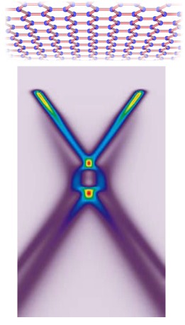
Graphene, a Manchester University discovery, is a material comprising sheets of carbon just one atom thick; graphene is like a single layer of graphite. However, it was the discovery that it has some peculiar electronic properties because of the existence of massless quasiparticles that has led to an explosion of interest in this material. Some researchers suggest that ultimately it will become the material that gives us a post-silicon world in computing.
Now, US scientists have made the first observation of the energy bands of complex particles within graphene known as plasmarons. This small step is an important one in understanding graphene and using it to develop devices for that future of ultrafast chemical computers.
At Berkeley Lab’s Advanced Light Source, an international team led by Aaron Bostwick and Eli Rotenberg have shown that these composite plasmaron particles are vital in generating graphene’s unique properties. “Graphene’s true electronic structure can’t be understood without understanding the many complex interactions of electrons with other particles.”
The electric charge carriers in graphene are negative electrons and positive holes, which in turn are affected by plasmons, oscillations in the density of the material that travel like sound waves through a sea of electrons. A plasmaron is “simply” a charge carrier coupled to a plasmon. “Although plasmarons were proposed theoretically in the late 1960s, and indirect evidence for them has been found, our work is the first observation of their distinct energy bands in graphene, or indeed in any material,” Rotenberg says. The team reported details of their findings in the journal Science in May.

The relationships between charge carriers, plasmons, and plasmarons will be important in the development of plasmonics, the architecture analogous to electronics in conventional silicon semiconductor circuitry. An important aspect of studying these relationships is to produce flat graphene sheets; graphene is usually rumpled like unmade bed linen. “One of the best ways to grow a flat sheet of graphene is by heating a crystal of silicon carbide,” Rotenberg explains, “and it happens that our German colleagues Thomas Seyller from the University of Erlangen and Karsten Horn from the Fritz Haber Institute in Berlin are experts at working with silicon carbide. As the silicon recedes from the surface it leaves a single carbon layer.”
With flat graphene sheets in hand, the team used a beam of low-energy, or soft, X-rays to analyse the materials. The resulting data provided them with an image of the electronic bands created by the electrons themselves. Even from the initial experiments, the team suspected graphene’s behaviour was more complicated than simple theory would suggest and seemed to hint at the existence of bare electrons. Since bare electrons cannot exist, the researchers postulated the fuzziness in their image was due to charge carriers emitting plasmons. Additional experiments with graphene sheets isolated from their support material revealed that electrons detached by the X-rays can leave behind either an ordinary hole or a hole bound to a plasmon – a plasmaron, explains Rotenberg.
“By their nature, plasmons couple strongly to photons, which promises new ways for manipulating light in nanostructures, giving rise to the field of plasmonics,” Rotenberg says. “Now we know that plasmons couple strongly to the charge carriers in graphene, which suggests that graphene may have an important role to play in the merging fields of electronics, photonics, and plasmonics on the nanoscale.”