Seth Marder of the Georgia Institute of Technology discussed details of the two-photon 3D lithography technique, at the annual meeting of the American Association for the Advancement of Science (AAAS) in Seattle. Two-photon 3D lithography is a disruptive platform technology that we believe will provide broad new capabilities, says Marder, We believe this technique provides a real competitive advantage for making complicated three-dimensional microstructures.
The technique relies on the unique properties of bis-donor phenylene vinylenes, which can absorb two photons of light simultaneously, to achieve an excited state. Once excited, the molecules transfer an electron to form a simple acid or a radical group that can initiate a chemical reaction – such as polymer cross-linking or ion reduction. It is these reactions that can change the internal structure of a resin slab containing monomer and doped with phenylene vinylene.
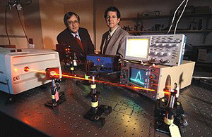
Researchers Seth Marder (left) and Joseph Perry pose with a laser system that can write 3D microstructures in polymeric materials. (Credit: Georgia Tech Photo: Gary Meek)
A computer-controlled laser beam would then be used to draw the required structure. At the focal point photons would initiate the cross-linking reactions. The unconverted parts of the slab could then be removed by solvent leaving the insoluble cross-linked 3D structure.
The molecules developed by Marder and colleague Joseph Perry are far more efficient than other photoactive materials, which means 3D structures can be formed in a polymer slab just 100 micrometres thick. Crucially, the laser light intensity needed is sufficiently low that the materials themselves are not damaged.
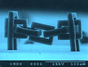
This microchain structure fabricated with the two-photon 3D lithography process is an example of a structure that would be difficult to produce layer-by-layer with 2D lithographic processes. The links are topologically connected, but not directly anchored to the surface.
The process exploits the fact that laser intensity is highest at the focus of a beam allowing two-photon activated chemistry to be localized at a very precise point. We can define with a very high degree of precision in the x, y and z coordinates where we are getting excitation, Marder explained. Using 700-nanometer light, the patterning precision can be about 200 nm across by 800 nm in depth. The requisite two photons will be available only at this focal point, so the chemical reactions are triggered only at these positions.
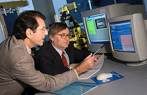
Researchers Joseph Perry (left) and Seth Marder examine test results for 3D microstructures produced in polymeric materials using their new process. (Credit: Georgia Tech Photo: Gary Meek)
The technique is not limited to polymers and Perry and Marder are using it to make tiny silver wires from patterns written in materials containing silver nanoparticles and ions. One such structure they have created is a microchain structure. This would be very difficult to create using the conventional tools of the microelectronics industry, such as 2D lithography, which involves building up a structure by etching away semiconductor layer by layer processes.
The precise control possible with modern lasers means that the researchers can switch it on and off very precisely too. They can thus create almost any three-dimensional shape in the resin slab, including moving parts, such as gears and chains. The team adds that the 3D polymerised structures are currently made one at a time and so might themselves be used as moulds for mass production of other structures in a more useful material, through a simple stamping processes.
However, the team is working on integrating technologies so that they can increase operation speed to a thousand times that of the current setup. A single 3D fabrication system should be able to generate about a million individual device structures per day. With a production facility using a number of fabrication systems, there is potential for certain types of mass production, says Perry. The technique could also be used to create surfaces with particular textures. These could be tailored to act as scaffolds on which living tissues might be grown.
Further reading
Seth Marder
http://www.chemistry.gatech.edu/faculty/Marder/
Joseph Perry
http://www.chemistry.gatech.edu/faculty/Perry/
Previous Spotlight article on Marder and Perry
http://www.intute.ac.uk/sciences/spotlight/issue4/acidity.html
Suggested searches
Photochemistry