Microscopic printing techniques could be used to make the next generation of electronic components for large-area displays with higher definition and covering much larger areas than currently possible, and much more versatile sensors for a range of applications from the environmental to the medical, all at dramatically reduced costs compared to current micromanufacturing technology.
Researchers can already carry out microcontact printing on metal surfaces a few tens of square centimetres in size using microcontact printing and etching. However, while this is a fairly straightforward approach on smaller areas, researchers would prefer to be able to develop a much simpler method applicable even to large-scale production for bigger displays and sensor arrays. Now, a team at Philips Research in Eindhoven in the Netherlands has developed what they call a universally applicable ink for microcontact printing.
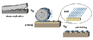
Microcontact printing process (Burdinski/Philips Research)
Microcontact printing involves making an elastomeric mould, essentially a rubber stamp made from polydimethylsiloxane or a similar material, but with patterning and features on the microscopic scale. The stamp is then loaded with an ink, which is then pressed on to the metal surface to be printed. The ink sticks to the metal surface, forming a monolayer of its component molecules in the microstructure pattern of the stamp. The process occurs because the molecules are designed to self-assemble into an ordered arrangement. The molecules provide a resistant layer for the next step, which involves applying a corrosive, etching agent. The coated areas are protected from etching and so only exposed metal is removed. Once the etching process is complete, the protective monolayer can be dissolved away using a solvent that doesn’t affect the metal. The product is an inverse version of the rubber stamp.
Coinage metals and materials, such as silicon and aluminium, which have an oxide surface, can be patterned in this way but each type of surface requires a different type of ink to stick to it. Gold and related metals need a sulphur-containing compound to form metal-sulphur bonds to anchor the monolayer while phosphonic acids can be used for aluminium or semiconductors. Another problem arises if one wishes to use the same rubber stamp to pattern two different materials in the same manufacturing process as the ink cannot be washed off and a new one applied easily.

Dirk Burdinski
Dirk Burdinski and colleagues at Philips have now developed an ink for microcontact printing that simply consists of a mixture of both types of ink, sulphur-containing octadecanethiol and octadecanephosphonic acid. When polydimethylsiloxane stamps are loaded with this ink, metals, semiconductors and oxidic metals can be patterned. The individual components of the ink are selectively transferred to their corresponding surface without interfering with each other.
The universal ink also has great potential in microfluidic, or lab-on-a-chip systems for diagnostic devices, as these are often made of different materials which so could be surface-modified or patterned by applying the mixed ink. Philips Research is also developing a new patterning technology, microcontact wave printing, based on this printing process for the manufacturing of liquid crystal displays and even fully printed all-plastic electronic circuits. The major benefits of this micro-printing technique are its simplicity and the potential for cost saving particularly in large area patterning, which is very expensive with conventional photolitho-technology, Birdinski told Spotlight. The technology may also be applied to the immobilization of biomolecules on sensor arrays or the modification of the inner surfaces of microfluidic devices, where no etching step is necessarily used.
Further reading
Angew Chem Int Edn
http://dx.doi.org/10.1002/anie.200600310
Philips Research
http://www.research.philips.com/