There seems to be no technology that nanotubes cannot slip into. Researchers are developing them as insulating sheaths to wrap around molecular wires for a future generation of nano-electronics. They already find themselves at the tip of high resolution scanning probe microscopes for taking a close look at tiny structures. And, in the more mundane-seeming world of lubrication, they are turning out to be rather slippery customers. Chemists too are hoping to use nanotubes as reaction vessels inside which novel chemistry could be forced to take place away from the bulky milieu of the standard solution in a glass reaction flask.
Until recently, nanotubes – hollow tubes of carbon that look like a microscopic roll of chicken wire – have tended to be rather strait-laced. The have been described as something half-way between a carbon fibre and the soccerball-shaped all-carbon C60, fullerene molecule.
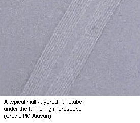
Nanotube
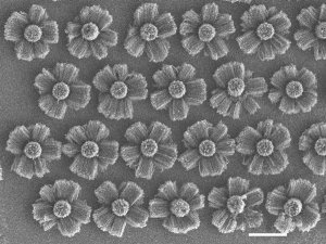
Now, a team at Rensselaer Polytechnic Institute in Troy, New York State, have created the next generation of carbon-based nanotubes that can be grown up, down, sideways, and in all three dimensions. This new world of nanoscale architecture could open up the possibility of 3D computer chips, integrated circuits, and the tiniest of chemical plants in the form of microelectromechanical (MEMS) devices.
Materials scientists Pulickel Ajayan, Ganapathiraman Ramanath and colleagues at Rensselaer point out that to be useful in devices nanoscale structures must be have well-defined architectures rather than being randomly positioned and pointing in all directions or only one direction. To build integrated systems of the kind needed for MEMS and electronics, there has to be control in the production of nanotubes.

Pulickel Ajayan
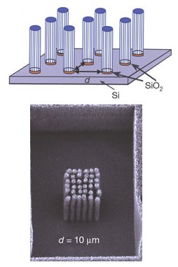
Ajayan and Ramanath have now brought together two different approaches to help them bring new control to the assembly of nanotubes. They have used a chemical-vapour deposition (CVD) method, in which vapourised carbon from an organic molecule, such as xylene, at 800 Celsius are allowed to condense on a silica surface to form the nanotubes.

Ganapathiraman Ramanath
They also use a gas-phase catalyst – a pentamethylferrocene – that can help direct the assembly of the carbon nanotubes. But, instead of allowing the catalysed CVD process to take its own course and result in vertically oriented tubes, they have coupled it with technology that allows them to etch the silica, using standard printing, microlithographic wet/dry techniques from the electronics industry.
More nanotubes
With this templated surface in place, the growing multiwalled nanotubes have no option but to adopt predetermined orientations on the surface. This has allowed the team to build one-, two- and three-dimensional arrangements of nanotubes. It’s a simple and elegant process that provides unprecedented control over nanotube growth, said Ajayan.
Nanotube process
The team reckon that what they describe as essentially a simple process for controlled nanotube growth will be brought to market in the next few months for further development by the MEMS and electronics industries hoping to develop lab-on-a-chip devices and other such microscale machines. Our fabrication method can be scaled up to large areas and is compatible with standard silicon microfabrication technology, adds Ajayan.
Ramanath is enthusiastic that the process will be taken far beyond nanotubes. This is the first step toward controllably making complex networks comprised of wire-shaped molecular units, he explains, By manipulating the topography of the silica blocks, and utilizing the selective and directional growth process, we have been able to force nanotubes to grow in predetermined, multiple directions, with a very fine degree of control. No one else has done this.
Further reading
Nature, 416, 495-496 (2002)
DOI: 10.1038/416495a
Suggested searches
Microelectromechanical systems
Nanotubes